DACG Photo Gallery
The front page of the magazine of the DACG, the FACET , each time shows an image that has a special meaning within crystal growth. You can send your favorite figure, accompanied by an adequate description, to the editors by electronic mail. The editor chooses the most beautiful illustration from the entries, entirely according to his own taste. This is placed on the cover of the FACET , with the description and source reference on the inside page. The images also appear here, in the DACG Photo Gallery. Because of the good accessibility via the internet, the images are compressed to a size of up to 150 kB.
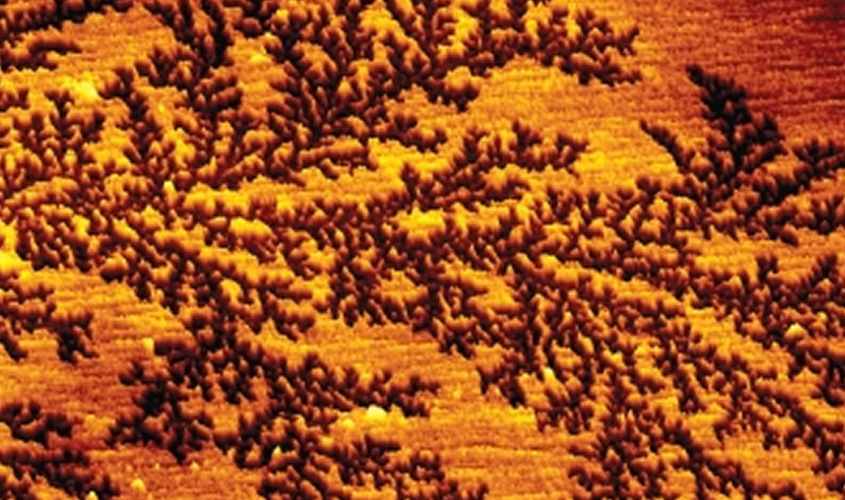
The figure was provided by Pantelis Bampoulis, Harold Zandvliet, Detlef Lohse and Bene Poelsema from the University of Twente.
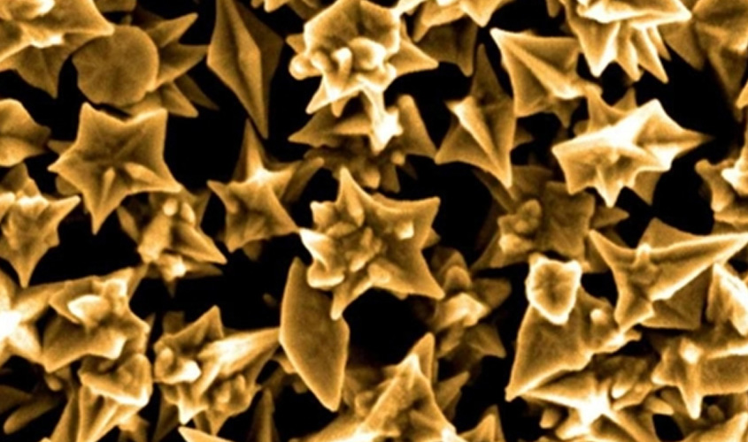
The optical properties are highly dependent on the shape and size of the nanoparticles. The characteristic optical resonance is thus adjustable over a wide spectral range, from visible to near infrared.
The figure was provided by Waqqar Ahmed and Stefan Kooij of the University of Twente.
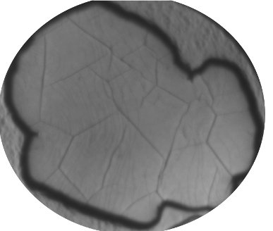
A Low Energy Electron Microscopy (LEEM) image of a graphene crystal grown on an Ir(111) surface. The graphene layer is 1 atom thin and is widely seen as a future material for manufacturing electronic circuits with improved properties compared to Si. A line structure is visible in the crystal. These are partly atomic step edges of the underlying substrate that are visible through the graphene. More clearly, a number of thick lines can be seen on the graphene. These are wrinkles that have arisen as a result of stress that arises after cooling the graphene from the growth temperature to room temperature.
The figure was provided by Raoul van Gastel of the University of Twente.
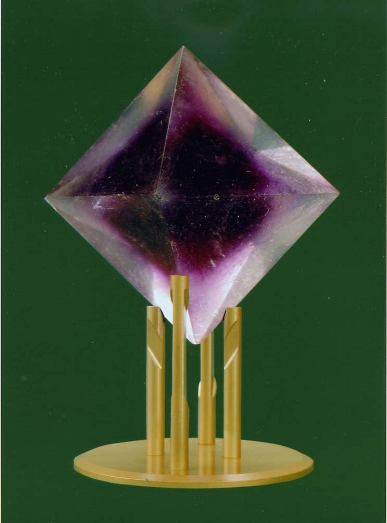
An alum crystal grown by Rik Wagenaar. It is an almost perfect octedral crystal of great clarity. Wagenaar had started with chrome alum, but had switched to aluminum alum to keep costs down. His crystal therefore shows a hazy purple core. Wagenaar’s unparalleled technique comes down to crystallization by evaporation at room temperature. That is to say: at the lowest possible room temperature. That is why Wagenaar preferred to work in the winter and in dry weather. His crystal measures 162.5 mm (largest diagonal) and weighs 1,299.23 grams (measurements were made at the University of Groningen). (See also: Europhysics News 40 (1) 5, 2009. Online: www.europhysicsnews.org).
The figure was provided by Henk Kubbinga of the University of Groningen, EPSHistory of Physics Group, with thanks to Jeff de Hosson, RUG Chair of Materials Science.
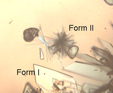
The stable form I (plate-like) and metastable form II (needles) of a co-crystalline compound of 1:1 Carbamazepine and Isonicotinamide. Both crystals appeared during a solvent-mediated transformation of the pure component crystals in ethanol. While the pure component crystals dissolve, both co-crystal forms appear. Eventually, form I remains at the expense of form II (JH ter Horst, PW Cains, Crystal Growth Design 8(7) (2008) 2537).
The figure was provided by Joop ter Horst of Delft University of Technology and Peter Cains of Avantium Technologies.
A Low Energy Electron Microscopy (LEEM) image of a bismuth overlay structure on a Cu(111) substrate. The bright areas of the zebra structure are covered with a liquid Bi monolayer and the dark areas consist of a surface alloy of Bi with the copper substrate. The picture was made during an experiment in which heating causes the surface alloy to lose its long-range order. This leads to the formation of the triangular domain structures that interrupt the zebra structure in the picture shown.
The figure was provided by Raoul van Gastel and Bene Poelsema from the University of Twente and Daniel Kaminski and Elias Vlieg from Radboud University Nijmegen.
Pt atomic chains on a Pt modified Ge(001) substrate, viewed with STM at room temperature (Bias voltage ~ 1.5 V, tunnel current 0.45 nA). The Pt was deposited at room temperature in UHV via resistive heating of a W filament wrapped with Pt. The Pt atoms first mix with the Ge substrate, but appear as atomic chains on the surface after an annealing step at high temperature. The atomic Pt chains are literally free of kinks and defects, and have lengths up to several hundred nanometers.
More information can also be found in the following journals:
Applied Physics Letters 83(22), 4610-4612 (2003)
Physical Review Letters 95(11), 116801 (2005)
Nano Letters 6(7), 1439-1442 (2006)
Nanotechnology 18(36), 365305 (2007)
The figure was provided by Arie van Houselt and Harold Zandvliet of the University of Twente.
Crystals of table salt grown through the gas phase. This photo, taken by Wim Noorduin and Sander Graswinckel of IMM Solid State Chemistry, Radboud University Nijmegen, was the winner of the photo competition at the BACG/DACG meeting in Edinburgh, September 2006.
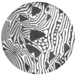
A Low Energy Electron Microscopy (LEEM) image of a self-assembled maze structure of Pb deposited on a Cu(111) surface. The deposited lead forms both a surface alloy (dark) and an overcoat structure (light). The two surface structures have different surface tensions, which leads to the self-assembly of the maze pattern shown in the picture. The length scale of the image is 1.7 μm.
Figure provided by Raoul van Gastel of the University of Twente .
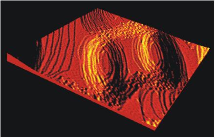
Growth spirals on tetracene. On the left the experimental shape as observed using an atomic force microscope, on the right the prediction via a computer simulation.
Figure provided by Herma Cuppen of the Radboud University Nijmegen .
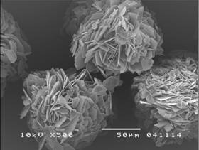
An SEM image of L-glutamic acid: platelets of the stable beta phase are visible. This phase has nucleated and grown from (probably) a metastable droplet, created as a result of liquid-liquid separation. The segregation has been observed during pH-shift crystallization at high supersaturation in a premixed solution, but not a post-stirred crystallizer.
Figure provided by Marc Roelands of TNO .
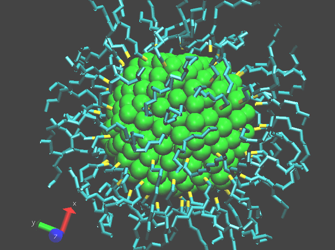
Computer simulation of a gold nanocrystal (NC). Its core consists of 309 gold atoms (shown as green spheres), in an icosahedral equilibrium structure. The core is capped with 80 thiol molecules (HS-(CH2)9-CH3), the sulfur atoms are colored yellow. The reasons of capping a NC are (1) to control the interactions between NCs, (2) to control the growth during colloidal synthesis, and (3) to passivate dangling bonds to prevent nonradiative recombination of electrons and holes at the surface. Computer simulations are used to investigate the influence of the capping layer on the interactions between NCs and on their self-assembling properties.
Figure provided by Thijs Vlugt and Jan van der Eerden of the Utrecht University .
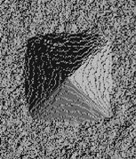
A computer simulation of a pyramid that can be created during the etching of silicon. Such pyramids are undesirable in practice. For this research, Dr. Erik van Veenendaal received the Crystal Growth Prize 2002 on 8 November 2002. The research was carried out at the Department of Solid Substance Chemistry of Prof.dr. E. Fly and Dr. WJP van Enckevort of the Catholic University of Nijmegen, in collaboration with the Department of Micromechanical Transduction Technology of Prof. dr. M. Elwenspoek of the University of Twente.
Figure supplied in 2003 by: Erik van Veenendaal, Elias Vlieg and Willem van Enckevort, Catholic University of Nijmegen .
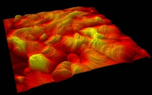
Polycrystalline gold film, taken with the scanning tunneling microscope (STM). The 30 nm thick film was deposited on a quartz substrate in an ultra-high vacuum system at room temperature. The atomic steps shown in the 350 × 350 nm picture 2are clearly visible, indicate that the thin layer consists of a collection of fairly randomly oriented crystallites. Due to this structure, the layer is very rough. By following the layer during heating from room temperature to 440 °C with the variable-temperature STM used, it was possible to demonstrate that the roughness first decreases and then increases again. This astonishing variation could be fully explained by changes in the orientations of the crystallites and their grain boundaries, and by the average size of the grains. This work is published in Phys. Rev. Lit. 91 (2003), 026101 .
Figure provided in 2002 by: Marcel Rost, Dennis Quist, and Joost Frenken, Leiden University .
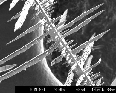
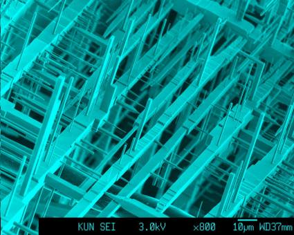
Escher’s table salt: By growing via sublimation and at high supersaturation, an intriguing network of dendritic NaCl crystals is created. This micrometre-scale 3-dimensional network bears a striking resemblance to some of MC Escher’s works. The crystals were grown by Wim Noorduin and Sander Graswinckel at the Solid State Chemistry Department of Willem van Enckevort and Elias Vlieg at the Catholic University of Nijmegen.
SEM photo supplied in 2003 by: Wim Noorduin, Sander Graswinckel, Willem van Enckevort and Elias Vlieg, Catholic University of Nijmegen .
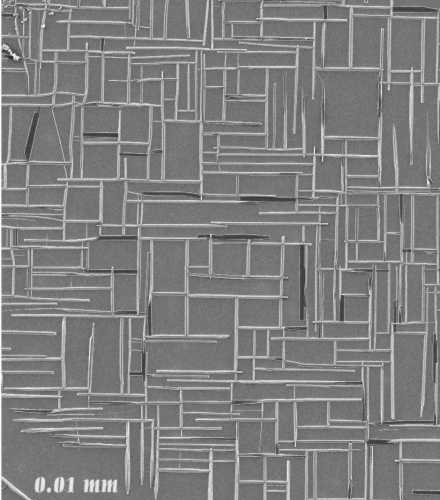
Crystallographic Mondrian recorded with the scanning electron microscope. Here we see oriented alizarin crystals (an organic dye) on a {100} NaCl substrate. The needle direction of the alizarin crystals point in the two symmetrically equivalent <011> directions. The crystals have grown by sublimation from the gas phase at a temperature of about 75 °C.
KUN’s Solid State Chemistry department recently started a project to study the epitaxial growth of organic crystals on inorganic substrates. Initially, this occurs through the growth of oriented three-dimensional seeds, which later grow together to form a single crystal. The major advantage of this method compared to the usual heteroepitaxis via the growth of closed films over the entire surface is that the lattice parameters of the substrate and the grown layer may deviate by a few percent (up to 10%). The intention is to grow larger crystals in this way from materials that normally do not crystallize. In addition, new polymorphs can be force-nucleated in this way.
Figure supplied in 2002 by: Sander Kleine, Mirjam Leunissen and Willem van Enckevort, Catholic University of Nijmegen .
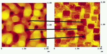
Atomic force microscope image of the surface of a layer of YBa 2 Cu 3 O 7-d on a substrate of SrTiO 3 . On the left the surface immediately after its creation, on the right after five seconds of etching. Pits have formed around islands.
There appears to be a direct relationship between the amount of defects and the strength of the magnetic field at which the critical current density is maximum. That these linear defects pin the vortices so well appears to be because the linear defects and the vortices are parallel to each other and are of the same order of magnitude. As a result, the vortices are held over their entire length. The linear defects arise naturally and appear to be ordered (the pitting pattern created by the dissolution is very regular). Trials to artificially introduce such defects yielded less good results because the defects do not arise in an orderly fashion.
Figure supplied in 2001 by: Jeroen Huijbregtse and Bernard Dam , Vrije Universiteit Amsterdam
In-situ Scanning Tunneling Microscope (STM) image of the (110) surface of a gold crystal. The surface has been artificially roughened by a combination of ion bombardment and heating on a scale of tens to hundreds of nanometers. Each of the fine lines is an atomic step on the surface. Due to the special atomic stacking of this surface, in a so-called “missing-row” reconstruction, the steps are forced to adopt very unusual structures. As a result, the mountains and valleys develop an “almond” shape, characterized by two curved sides, connected on both sides at an acute angle. Networks of intersecting steps are observed between the tonsils. Based on the formation energies of steps and kinks on this surface, the shapes can be explained quantitatively. This work was published this year in Phys. Rev. Lit. 84 (2000), 1966-1969 .
Figure supplied in 2000 by: Marcel Rost and Joost Frenken, Leiden University
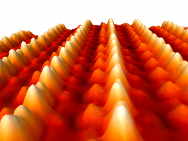
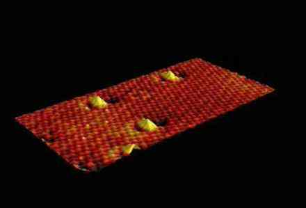
In-situ Scanning Tunneling Microscope (STM) image of the (001) surface of a copper crystal. The regular pattern of small bumps corresponds to the atomic lattice of copper atoms. The large bumps are indium atoms deposited in a vacuum system at room temperature. These indium atoms have spontaneously diffused into the outer atomic layer of the copper crystal. Each indium atom takes the place of one copper atom. The indium atoms allow the copper to grow on this surface layer by layer, rather than in the form of rough, three-dimensional growth. The indium atoms themselves appear to perform a miraculous diffusion motion within the outer copper layer, making “giant jumps” of several atomic distances.
Figure provided in 2000 by: Raoul van Gastel and Joost Frenken, Leiden University
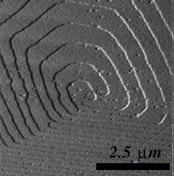
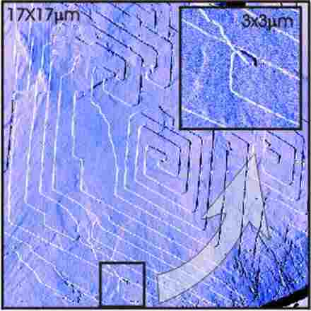
Ex-situ Atomic Force Microscope (AFM) image of the (001) surface of a solution-grown n‑C 40 H 82 crystal. An nC 40 H 82 paraffin molecule is an unbranched 5 nm long alkane chain with 40 C atoms. In the space group of these crystals, Pca2 1, the molecules are all parallel to each other; perpendicular to the (001) plane. The rhombic shape of the single and bifold spirals shown on the (001) plane reflects the space group symmetry. The steps on the surface are all mono-molecular. In addition to the straight spiral steps that have arisen during growth, irregular steps can also be seen. These irregular steps intersect the spiral steps and also intersect themselves, as shown in the inset. The cause of these wondrous step intersections is the displacement of dislocations after growing. External forces have moved some screw dislocations, leaving an irregular step trail. These tracks, which can cross existing step patterns,
Illustration provided in 2000 by: Marco Plomp and Peter van Hoof, Catholic University of Nijmegen .

